NVIDIA to Pioneer TSMC’s A16 Process for Next-Generation “Feynman” GPUs
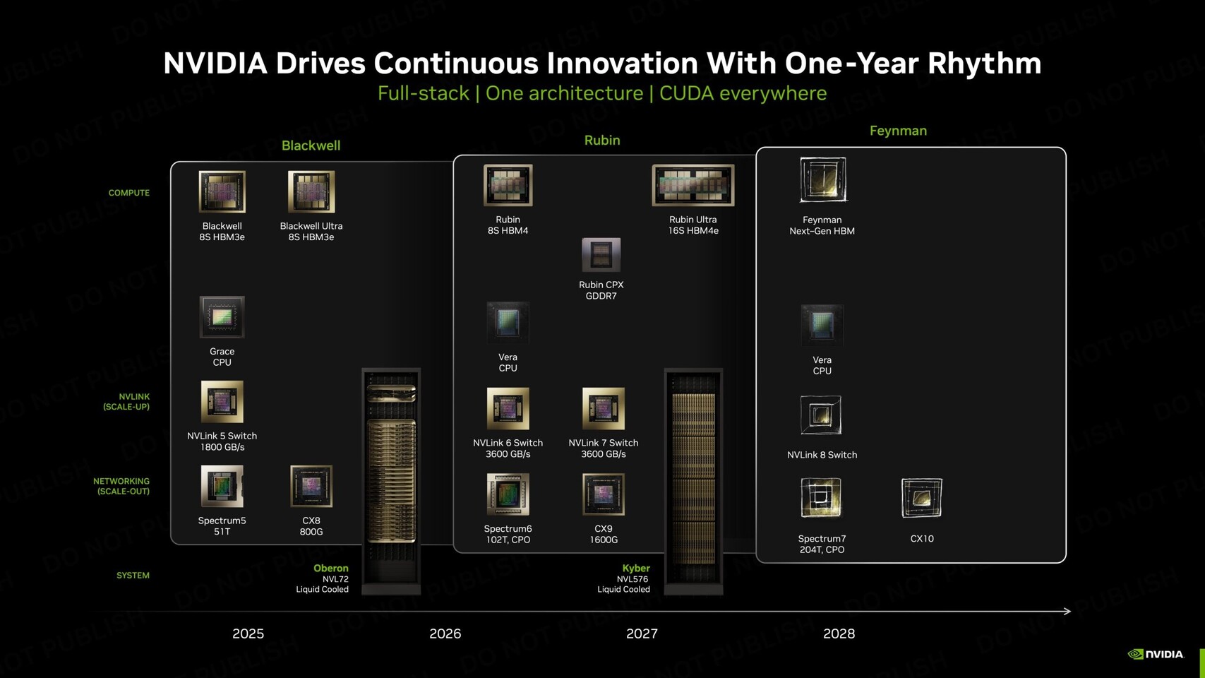
NVIDIA is set to make a pivotal shift in its GPU manufacturing strategy with its upcoming “Feynman” architecture, becoming the first customer to adopt TSMC’s advanced A16 process node. This move marks a departure from NVIDIA’s traditional approach of leveraging slightly older semiconductor nodes to maximize efficiency and performance for its datacenter accelerators.
Historically, NVIDIA’s largest AI chips, such as the current “Blackwell Ultra” with an impressive 104 billion transistors, have pushed the boundaries of chip design, often exceeding reticle size limits. These massive dies typically benefit from mature process nodes, which offer better yields and manageable thermal profiles. However, the surging demand for AI compute power is prompting NVIDIA to embrace the cutting-edge A16 node for Feynman, while other product lines like “Rubin” will continue to utilize refined N3P variants combined with CoWoS-L advanced packaging.
Advantages of TSMC’s A16 Node and Backside Power Delivery
The standout feature of TSMC’s A16 process is its innovative backside power delivery system. By separating power and signal routing, this technology reduces electrical losses and streamlines chip floor planning. Approaches range from buried power rails—still utilizing the front-side metal layer—to power vias that connect directly to the rear of the chip. TSMC’s Super Power Rail concept further enhances efficiency by delivering power straight to the transistor’s source and drain terminals, minimizing resistance and improving overall performance.
These advancements are particularly crucial as power requirements for high-end AI accelerators continue to escalate. The current Blackwell Ultra GPUs already consume around 1,400 watts, and the next-generation Rubin designs are projected to surpass 2,300 watts. Selecting the right process node is therefore essential for the Feynman architecture, which is expected to operate at multi-gigawatt power levels.
Looking Ahead: Timeline and Industry Impact
If TSMC’s A16 process achieves volume production as scheduled, the first Feynman silicon could debut as early as late 2027 or early 2028. This strategic adoption positions NVIDIA at the forefront of semiconductor innovation, setting new standards for AI hardware performance and efficiency in the datacenter space.