IBM Unveils World’s First Sub-1 Nanometer Chip with Revolutionary Nanostack Architecture
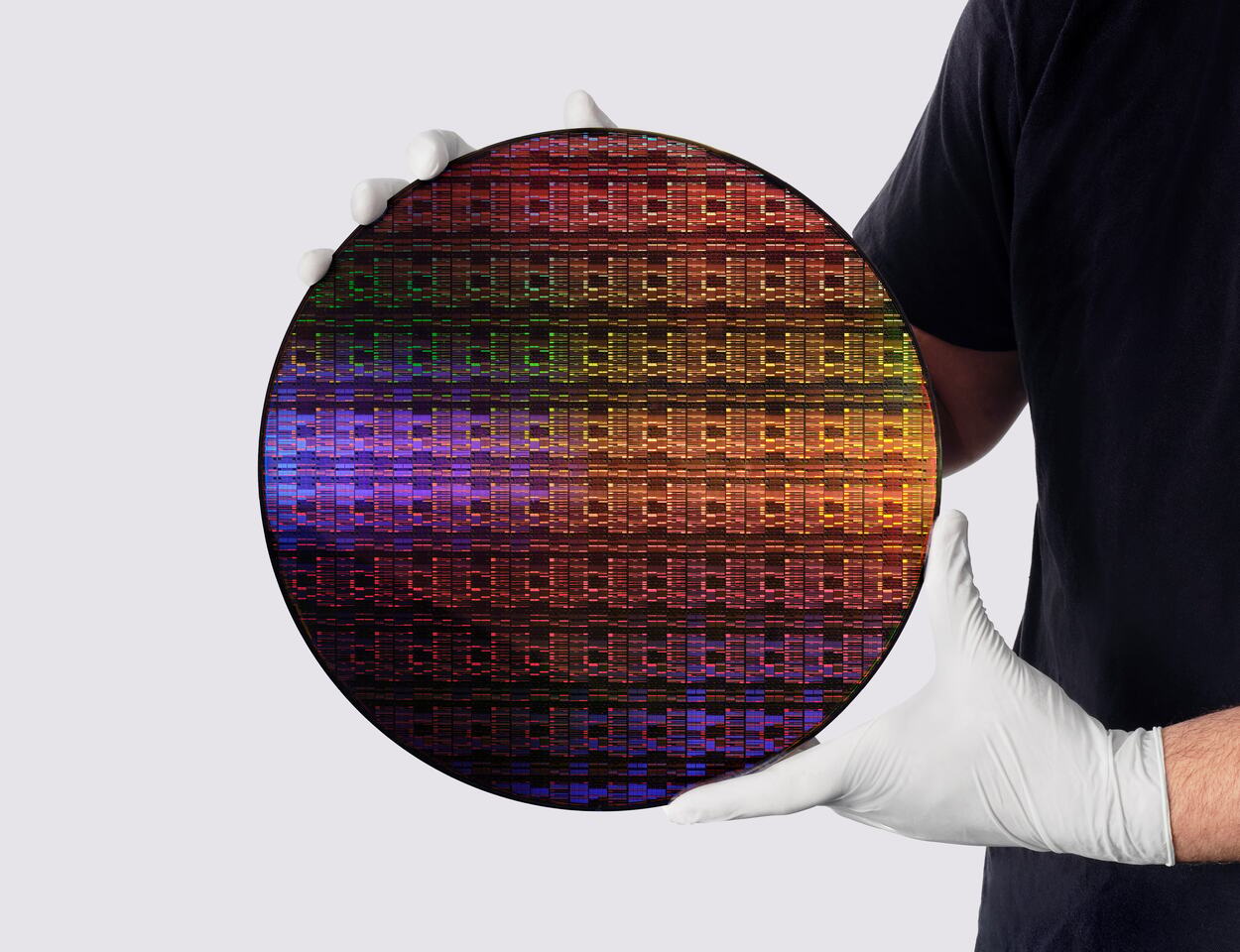
IBM has announced a significant milestone in semiconductor technology with the introduction of the world’s first sub-1 nanometer (nm) chip, featuring a groundbreaking transistor architecture at the 0.7 nm, or 7 angstrom, node. This achievement represents a pivotal advancement for the semiconductor industry, which has long grappled with the physical limitations of traditional chip scaling. Semiconductors are foundational to modern computing, powering everything from consumer electronics and communication devices to transportation systems and critical infrastructure.
Breakthrough in Chip Density and Performance
The new sub-1 nm chip from IBM integrates nearly 100 billion transistors onto a chip the size of a fingernail—almost double the density of IBM’s 2 nm chip introduced in 2021. This leap in transistor density is made possible by a series of innovations in both materials and chip structure, most notably IBM’s pioneering three-dimensional nanostack architecture. As chip features approach atomic dimensions, this technology demonstrates that further improvements in performance and energy efficiency are still achievable.
Technical results indicate that the new chip could deliver up to 50% higher performance or 70% greater energy efficiency compared to IBM’s 2 nm node chips. This advancement is poised to accelerate computing capabilities for a wide range of applications, including generative AI, cloud infrastructure, and next-generation electronic devices.
Introducing Nanostack: A New Era in Transistor Design
At the core of this innovation is IBM’s “nanostack” architecture—the industry’s first known three-dimensional, nanosheet-based transistor design. Nanostack builds upon and surpasses the current leading-edge nanosheet technology, also pioneered by IBM. By vertically stacking and staggering transistors, the nanostack design leverages 3D sequential integration to significantly increase transistor density. This approach also enables the use of different material combinations within each stacked layer, allowing for independent optimization of performance and power efficiency for each transistor.
The nanostack architecture has been experimentally validated through ultra-thin dielectric bonding in CMOS integration, demonstration of dual-channel engineering, and successful operation of functional CMOS inverters with expected switching performance. These results confirm that nanostack technology is not only theoretically sound but also physically realizable and capable of supporting real-world computation.
In research presented at VLSI 2026, IBM demonstrated that the nanostack architecture enables a 40% scaling improvement in SRAM, paving the way for more efficient chips that can meet the high-bandwidth data requirements of advanced AI workloads.
Advancing the Era of Angstrom-Level Scaling
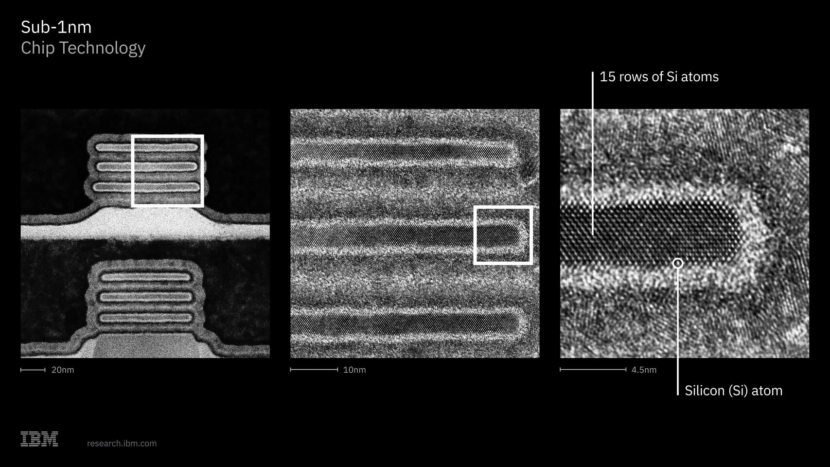
With the introduction of the nanostack structure, logic technology can now extend below the 1 nm node for the first time, ushering in the era of angstrom-level scaling where chip features approach the size of individual atoms. While modern transistor nodes refer to generations of manufacturing technology rather than exact physical dimensions, IBM’s 0.7 nm (7 angstrom) technology demonstrates that continued scaling is achievable. According to IBM’s semiconductor roadmap, the nanostack architecture supports at least another decade of progress in chip miniaturization.
IBM’s Legacy and Future in Semiconductor Innovation
This latest breakthrough reinforces IBM’s longstanding leadership in semiconductor research and development. From pioneering early semiconductors in the 1960s to introducing the world’s first 2 nm node chip, IBM has consistently driven advancements in silicon technology, AI hardware, logic, and quantum processors.
IBM’s semiconductor research is conducted at its advanced facility in Albany, New York, which is set to house a High Numerical Aperture Extreme Ultraviolet (High NA EUV) lithography tool—an essential technology for future logic scaling. Developed by ASML, High NA EUV enables ultra-precise circuit printing, facilitating the creation of smaller and more powerful chips. IBM collaborates with industry leaders such as Lam Research, Tokyo Electron, and SCREEN Semiconductor Solutions to develop new High NA EUV processes and tools, which have already produced working devices.
In addition, IBM recently announced the formation of Anderon, the world’s first pure-play quantum foundry. As a standalone company, Anderon will leverage IBM’s expertise in quantum computing and semiconductor manufacturing to help position the United States as a leader in quantum wafer production.
Looking Ahead: Path to Production
With the earliest adoption of nanostack technology anticipated at the sub-1 nm node, IBM envisions a path to production within the next five years. This innovation not only sets a new benchmark for the semiconductor industry but also lays the groundwork for the next era of computing, where performance and efficiency continue to advance at the atomic scale.